WRIGHT-PATTERSON AIR FORCE BASE, Ohio (AFRL) – A team of Air Force Research Laboratory, or AFRL, researchers partnered with Pennsylvania State University to publish an article in the February 2023 issue of the prestigious scientific journal ACS Nano.
The publication highlights an innovative method for manipulating and tailoring the optoelectronic properties of transition metal dichalcogenides, or TMDs, a specific class of two-dimensional layered materials essential for developing emerging sensing and electronic technologies. The research team’s findings have potential future applications for both the Department of the Air Force and the commercial market, said Dr. Rahul Rao, a research group leader in AFRL’s Materials and Manufacturing Directorate.

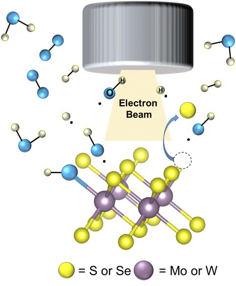
The graphic illustrates how the high-energy electron beam from a scanning electron microscope is used to functionalize transition metal dichalcogenides, or TMDs. Air Force Research Laboratory, or AFRL, researchers from the Materials and Manufacturing Directorate contributed this work to the February 2023 ACS Nano publication “Precision Modification of Monolayer Transition Metal Dichalcogenides via Environmental E‑Beam Patterning.” TMDs are a specific class of two-dimensional layered materials essential for the development of emerging sensing and electronic technologies for the Department of the Air Force and commercial market. The example shows hydrogen (H) and oxygen (O) atoms as they are added to TMD atomic layers consisting of sulfur (S), selenium (Se), Molybdenum (Mo) and tungsten (W) to functionalize them. The electron beam removes atoms from the TMD, causing a chemical reaction that emits light and heat which can be harnessed for use in sensing and other technologies. (U.S. Air Force graphic)
“Anywhere you might expect to see electronics in the future, you could find these materials,” Rao said. “This research has potential implications for use in quantum devices, satellite communications, aircraft, biosensing, vapor sensing. We wanted to be able to modify and control the properties of [TMDs] in order to know exactly what they can do so that we can make these devices.”
TMDs are comprised of ultrathin, two-dimensional layers of transition metals and chalcogenides — specific classes of elements found on the periodic table — that are only three atoms thick, said Dr. Ryan Selhorst, lead author and research scientist in AFRL’s Materials Development section of the Polymers and Specialty Materials branch.
Researchers used the focused, high-energy electron beam from a scanning electron microscope in a water vapor environment to create gentle chemical reactions on the surface of the TMDs. This process can be used to create high precision patterns, Selhorst said. The method chemically alters the TMDs’ structure and modulates their optoelectronic properties.
Functionalization is a process by which researchers add organic chemical functional groups, which are specific groupings of atoms within molecules with their own characteristic properties, to the TMDs, altering the thermal and optical properties of the material to be harnessed for use in sensing and other technologies.
Traditionally, scientists have used an intricate, time-consuming process called lithography to alter the electronic and optical properties of TMDs, Selhorst said. However, it can take researchers days or even weeks working in a tightly controlled, sanitary environment to complete the task.
“Traditional lithography is the basis of modern electronics. Researchers have worked for decades to get this kind of precision down,” Selhorst said. “But it is a multistep procedure. Your outcome relies heavily on the purity of the chemicals and the cleanliness of the room. You need pristine conditions, cleanroom suits — it’s a whole other ballgame.”
The method developed by Rao and Selhorst’s team alleviates the sanitation concerns and the need for multiple complex steps, Selhorst said.
“Using [our] process, you can generate any pattern that you would like, down to a resolution of 60 nanometers,” Selhorst said. “I can go in and do this whole procedure in roughly an hour, maybe a few hours at most.”
According to its webpage, ACS Nano publishes only original research that presents an advance of immediate, broad and lasting impact in the chemistry, physics, materials science, biology and engineering fields. Its impact factor — a universal ranking used to gauge the international reach and influence of peer-reviewed scientific journals — was approximately 18 in 2021.
Rao said the scientific community generally views any ranking above 10 as notable.

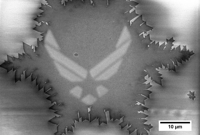
The image depicts a novel precision patterning method using the United States Department of the Air Force emblem on monolayer MoSe2, a two-dimensional material made of atomic layers. Air Force Research Laboratory, or AFRL, researchers from the Materials and Manufacturing Directorate contributed this work to the February 2023 ACS Nano publication “Precision Modification of Monolayer Transition Metal Dichalcogenides via Environmental E‑Beam Patterning.” The publication introduced an innovative process of altering and tailoring the optoelectronic properties of transition metal dichalcogenides, or TMDs. Researchers can control and manipulate the atomic properties of these materials to draw lines, shapes and desired patterns to demonstrate how the material’s thermal and optical properties can be manipulated for sensing and other technologies. (U.S. Air Force graphic)
“ACS Nano carries a lot of weight, particularly in the Materials Science community,” Selhorst said. “When researchers get published there, that’s a solid indicator that they’ve accomplished some significant scientific work. It’s pretty hard not to feel ecstatic about that.”
TMD research is a relatively new field that has only been active for about 10 years, said Rao.
“Research like this is always such a collaborative effort,” Selhorst said. “This whole project, the publication — none of it would have happened without [the entire team].”
Additional contributors from the AFRL Materials and Manufacturing Directorate’s Photonic, Electronic and Soft Matter Materials Division included researchers David Moore, Dr. Jie Jiang, Dr. Michael A. Susner, Dr. Nicholas R. Glavin, Dr. Ruth Pachter and Dr. Benji Maruyama. Zhuohang Yu and Dr. Mauricio Terrones from Pennsylvania State University’s Department of Materials Science and Engineering also contributed to the publication.
“Research teams sometimes can work as these incredibly well-oiled machines where everything just fits so perfectly into place,” Selhorst said. “This was one of those times. In simply doing our jobs, we created something absolutely astounding.”
Read the full publication at https://pubs.acs.org/doi/10.1021/acsnano.2c11503
About AFRL
The Air Force Research Laboratory, or AFRL, is the primary scientific research and development center for the Department of the Air Force. AFRL plays an integral role in leading the discovery, development and integration of affordable warfighting technologies for our air, space and cyberspace force. With a workforce of more than 11,500 across nine technology areas and 40 other operations across the globe, AFRL provides a diverse portfolio of science and technology ranging from fundamental to advanced research and technology development. For more information, visit www.afresearchlab.com.

