AFRL discovers technique for creating electronics using “Transformative Manufacturing”
WRIGHT-PATTERSON AIR FORCE BASE, Ohio – Electronic circuits, the backbone of modern electronic devices, require precise integration of materials in two- and three-dimensional space to control the flow of electric current. Traditional manufacturing of electronics requires expensive equipment, complicated processes, and are not readily customizable after purchase.
Imagine the possibility of designing your own electronics rather than having to buy them new. What if you needed a new radio antenna to operate at a different frequency than the one you currently have, or desire to create a sensor that could monitor your exposure to toxins, or require a capacitor/resistor network to better interface your Bluetooth speakers? Typically, this would require an entirely new system or electronic device.
On the horizon is a new technique using lasers to customize, design, repair and build electronics. Developed at the Air Force Research Laboratory, this laser “writing” technique allows the user to design and precisely place conducting, insulating and semiconducting materials with ease utilizing a substrate coated with a thin film. In this simple and elegant solution, the unstructured, amorphous film, a laser and the surrounding air are all that are required to drive the necessary patterning and local electronic property control needed for functional devices.
The report by scientists at AFRL and collaborators at UES Inc., Case Western Reserve University, University of Dayton, University of California at Los Angeles, and University of Cambridge appears in the journal Materials Today.
The group defines this new manufacturing strategy as “Transformative Manufacturing.” Unlike additive or subtractive manufacturing, where you are either adding or removing materials to make a functional device, transformative manufacturing requires a film and a laser beam to pattern electronic devices. The laser beam impacting the sample acts as a means to change the thin film through localized heating and causes reactions with the environment at extremely high temperatures.
The uniqueness of utilizing lasers lies in the ability to locally vary the intensity of light and exposure time, which precisely modifies the crystal structure and chemistry of the thin film in a location as small as one micrometer (much smaller than the width of a human hair). The amorphous film is then readily transformed into three different materials: semiconducting crystalline molybdenum disulfide, conducting molybdenum dioxide, and insulating molybdenum trioxide all with the precise conditions.
“Alternative strategies to pattern these materials outside of a cleanroom environment, have enabled rapid prototyping and eliminated design constraints imposed by traditional fabrication,” said Dr. Nicholas Glavin, Materials Scientist from the Air Force Research Laboratory. “Future development could see fully user-customized electronics.”
By modifying the laser pattern, individual electronic circuits can be designed on the fly with nearly complete freedom within the bounds of the manufacturing process. This is in contrast to traditional circuit design using thin film cleanroom processes, which can restrict reconfigurability, requiring expensive start-up equipment and a multitude of steps to complete.
“By engineering the architecture of the three different phases, electrical devices such as a resistor, capacitor and chemical sensor were laser-written directly within the precursor film, representing an entirely transformative manufacturing approach for the fabrication of electronic circuitry,” said Dr. Drake Austin, research scientist from UES, Inc.
Further optimization of film uniformity utilizing different laser sources and profiles is expected to result in highly controllable properties for future electronics and sensor devices. Additionally, exploring the transformative manufacturing technique utilizing optical sources to include flash lamps, parallel laser sources, laser holography and pulsed laser systems will significantly reduce the manufacturing time and increase the throughput and open new potential device architectures.
It is expected that by laser-processing these, or similar materials in active gases, various chemical reactions can be locally induced, possibly with the ability to access other chemistries/structures as well as new reaction intermediates for more complex circuitry.
The transformative manufacturing approach represents another instrument to add to the toolbox for manufacturing of novel electronic materials and devices, where the freedom of design and ease of manufacturing truly puts the user in the driver seat for customizable electronics.
The work was supported by the Air Force Office of Scientific Research. The article in Materials Today can be found at
https://www.sciencedirect.com/science/article/abs/pii/S1369702120303394.
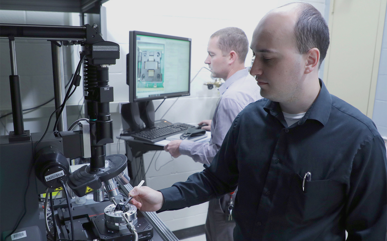
Researchers Dr. Drake Austin (UES, Inc.) and Dr. Nicholas Glavin (Air Force Research Laboratory) in the laser writing of electronics laboratory. (U.S. Air Force photo/Spencer Deer)
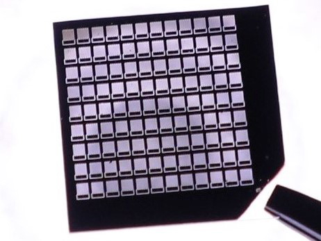
Close-up image of a laser-written capacitor network. (U.S. Air Force photo/Spencer Deer)
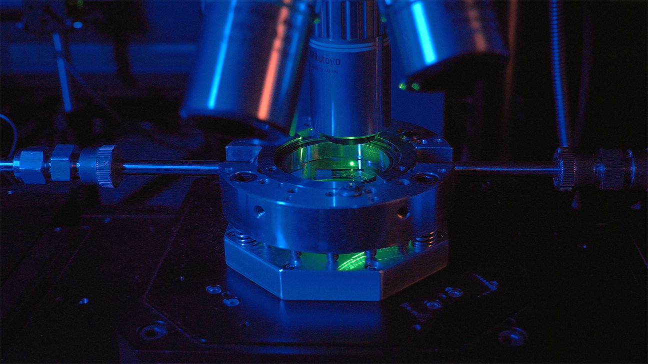
Laser writing of electronics utilizing a green laser and custom environmental chamber setup. (U.S. Air Force photo/Spencer Deer)