
WRIGHT-PATTERSON AIR FORCE BASE – Nanomaterials continue to amaze scientists and engineers with their astounding properties for future sensors and electronics, making them faster, better performing and wearable on a human.
Nanomaterials that arrange into a single atom-thick sheet, known as two-dimensional materials, are some of the more promising and influential to date. Researchers at the Air Force Research Laboratory, in partnership with UES Inc., University of Dayton, Rice University and the University of Pennsylvania, are exploring enhanced methods to characterize the state of these nanomaterials.
While “ideal” two-dimensional materials will realize atoms arranged into a perfect lattice structure practically, that is not the reality. In most cases, these materials are plagued with defects such as missing and disheveled atoms, internal grain boundaries and more. While this can be detrimental to performance, these imperfections can be useful.
The inconsistent uniformity and defects have proven beneficial in the cases of quantum emission, electronic transport control and improved accelerated chemical reactions.
“Regardless of the intended use, understanding and evaluating these defects is critical,” says Dr. Nicholas Glavin, research scientist at the Air Force Research Laboratory. “Even more vital, are developing characterization strategies that are both quantitative, nondestructive, and able to reach size-scales of the defects themselves.”
Researchers gained new insight into nanoscale features of a two-dimensional material known as molybdenum diselenide (MoSe2) by correlating electronic states using Kelvin probe force microscopy (KPFM) to optical states using tip-enhanced photoluminescence (TEPL). These two techniques utilize a nanoscale tip (~10 nm in size) to contact the 2D material and investigate both the electronic and optical properties.
The combination of KPFM and TEPL uncover hidden features in the MoSe2 to as small as 20 nanometers, or 1000 times smaller than a human hair.
“Invisible” nanoscale features including internal grain boundaries, oxidative regions and variations in chemical state all invisible to topographical mapping, providing insight into local chemical and excitonic states within the material. These results are highlighted in npj 2D Materials and Applications.
“The insights brought about using these techniques are invaluable for scientists to comprehend the activity in these materials,” says David Moore, research scientist at UES, Inc., one of the primary authors of the study. “Often, these nanoscopic features, invisible to the naked eye or even an optical microscope, drive the exciting material properties of two-dimensional materials.”
“Correlating nanoscale optical properties to electronic properties is one of the successes of this study and is a focus of our group,” said Prof. Deep Jariwala, co-corresponding author and Assistant Professor Electrical and Systems Engineering, the University of Pennsylvania. “This has been difficult to accomplish in a non-destructive manner, in the past.”
The KPFM and TEPL tools are used to track properties over time including the effect and mechanism of oxidation. As these materials age, their properties change due to a reaction with the environment.
“We are able to correlate local electronic states caused by oxidation and defects to unique optical states,” said Kiyoung Jo, doctoral candidate, from the University of Pennsylvania. “Since we resolved optical and electronic states to different locations and oxidation states in the 2D materials, this work will be impactful to future research in electronic devices, catalysis and energy devices.”
The collaborative work between AFRL, UES Inc., University of Dayton, Rice University and University of Pennsylvania has added another tool to the toolbox to examine nanoscale defects and imperfections in nanomaterials in their quest to improve resolution and quantify results for properties in Air Force applications.
The work was supported in part by the Air Force Office of Scientific Research and the article in npj 2D Materials and Applications (https://www.nature.com/articles/s41699-020-00178-w).
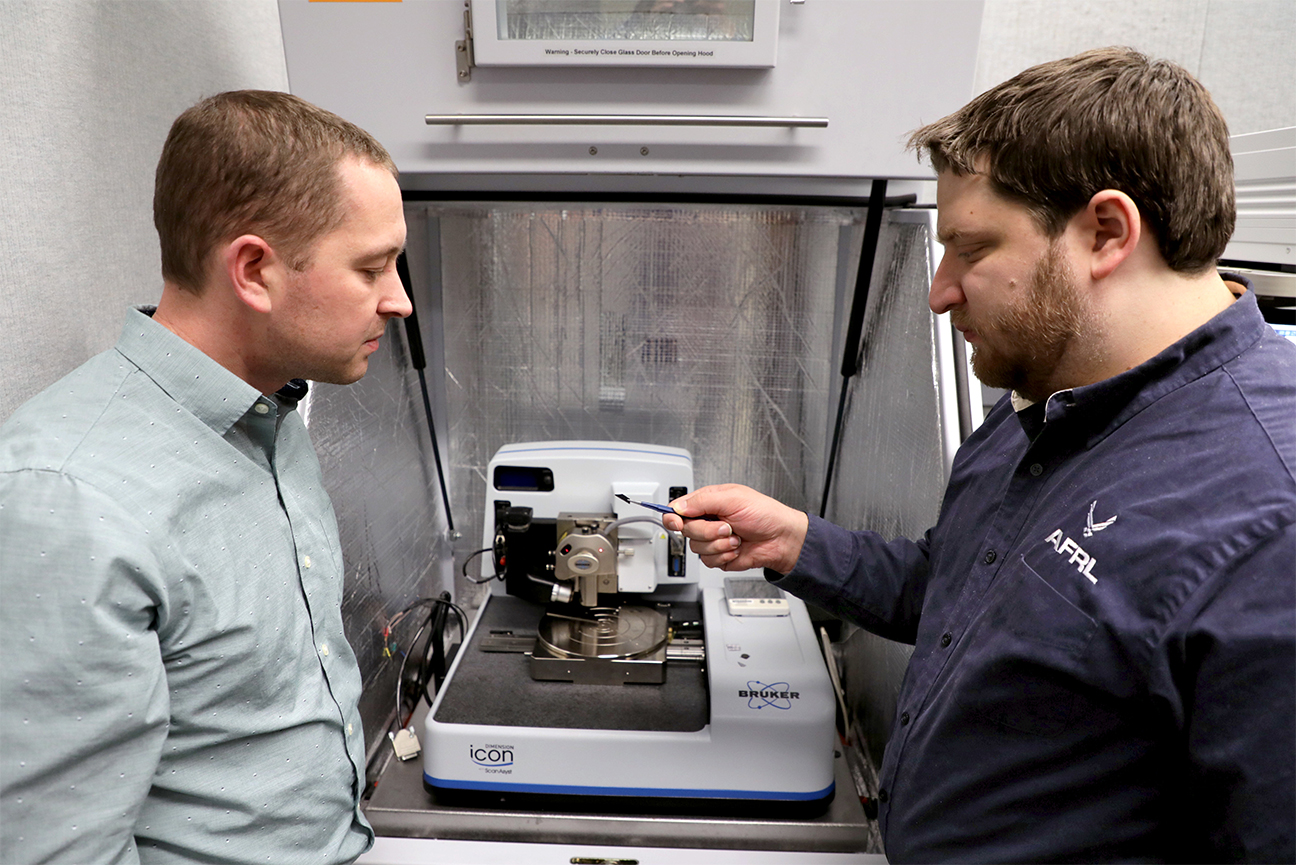
Dr. Nicholas Glavin, (left) research scientist at the Air Force Research Laboratory and David Moore, research scientist at UES, Inc. loading the sample into the analysis chamber. (U.S. Air Force photo/Spencer Deer)
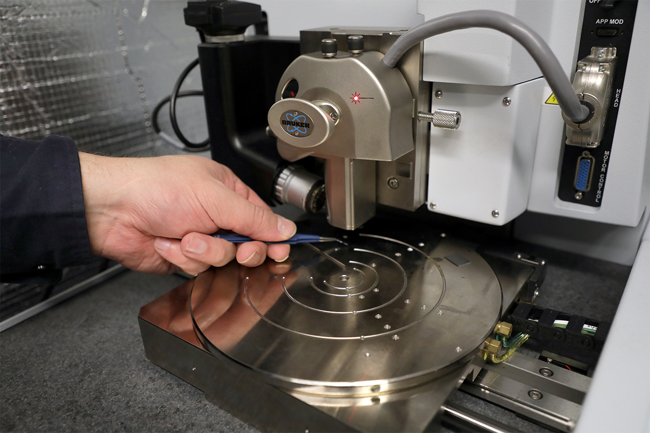
A sample is loaded into the Bruker Atomic Force Microscope system capable of performing nanoscale imaging experiments. (U.S. Air Force photo/Spencer Deer)
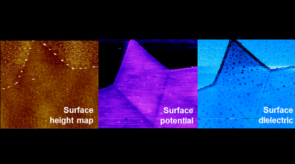
Atomic scale images (images are 40 micrometers x 40 micrometers) of surface height, surface potential and surface dielectric, in two-dimensional MoSe2 films, revealing many features invisible to traditional characterization methods. (U.S. Air Force photo/Spencer Deer)